Green nanotechnology and Sustainability

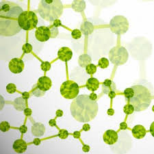
Everybody knows what is nanotechnology, it is the study and control of matter at the nano-scale, rearranging atoms and molecules. Nanotechnology has made marvelous contributions in the world of science especially in computer science and medical science.

But have you heard of green nanotechnology? The name itself suggests that it has something to do with greenery. It is the study of how nanotechnology can benefit the environment, such as by using less energy during the manufacturing process, the ability to recycle products after use and using Eco-friendly materials.

It builds on the principles of green chemistry and green engineering, and focuses on using the unique effects that occur in nano-scale materials.

Green nanotechnology can help to provide clean water to billions of people via novel filtration techniques, and has the ability to decontaminate dirty water. It can help in increasing the use of renewable energy and help in waste management too.

It can also influence the design of nano-materials and products by eliminating or minimizing pollution from the production of these materials.

It is all about making green nano-products and using them in support of sustainability. Sustainable development refers to a development that meets the needs of the present of the present, without compromising the ability of future generations to meet their own needs. It will aim at producing nano-materials without harming environmental or human health.

Nanotechnology can help reduce agricultural waste and bring down pollution levels. Scientists are working on nano-engineered enzymes that will allow simple and cost-effective conversion of cellulose from waste plant parts into ethanol.

Another example is rice husk that can become a source of renewable energy with nanotechnology. When rice husk is burned into thermal energy or bio-fuel a large amount of high quality nano-silica is produced, which can be further utilized to make other materials such as glass or concrete.

Nano sensors dispersed in the field can also detect presence of plant viruses and the level of soil nutrients.

Nanotechnology can reduce manufacturing costs for solar cells as a result of using a low temperature process.

Nanotechnology is being hailed as the next sunrise industry for India. The Department of Science and Technology of the Central Government has announced a national initiative in nano-materials, while the Jawaharlal Nehru Center for Advanced Scientific Research, Bangalore, has pioneered the study of nanotechnology in India. Prof. C.N.R Rao and the center has done world class research in nanotechnology using state of the art equipment.

A stream of nanotechnology-based products is beginning to emerge in India, with applications in the security realm. Besides D.R.D.O. (Defense Research & Development Organization) serious researches are also taking place in institutions like IIT, and Madras University.

Hopefully, in the near future as we advance further in the field of green nanotechnology, it will help us in replacing existing products with Nano-products that are more environment friendly.

INST scientists find route to fabricate precisely controlled nanostructures

Researchers at Institute of Nano Science and Technology (INST) Mohali, an autonomous institute under the Department of Science & Technology (DST) have found a straightforward and unique route to fabricate precisely controlled nanostructures of desired geometry and location on 2D materials, through a rapid one-step low power laser writing process.

Approaches used so far to achieve the controllability over hotspots distribution, which involves the synthesis of complex morphologies, limits their potential to be used for large area substrates. 

In order to overcome this, the INST group developed a hybrid Surface-enhanced Raman spectroscopy(SERS) platform of Molybdenum disulfide (MoS2) nanostructure decorated with gold nanoparticles, where direct laser writing is used to engineer the artificial edges on the surface of MoS2. This created localized hotspots with remarkable precision and control. Surface-enhanced Raman spectroscopy (SERS) is a technique for molecular detection and characterization that relies on the enhanced Raman scattering of molecules that are adsorbed on SERS-active surfaces, such as nanostructured gold or silver.

In the research by Dr. Kiran Shankar Hazraand his group which has been accepted for publication in the journal ACS Nano,a focused laser beam of meager power of a conventional Raman spectrometer was used to do nanostructuring on 2D flakes of desired feature size and geometry just by playing with the laser power and exposure time. Using this technique, they achieved the minimum feature size of   ̴300nm, which is close to the diffraction limit of the laser used (i.e., 532nm laser line). 

In SERS sensing, producing SERS substrate of controllable hotspots distribution with desired geometry and location is the main challenging task. Several efforts have been made by researchers to attain the controllability over hotspots distribution via employing various synthesis procedures, hotspots engineering, defect engineering, and so on. However, the random distribution of hotspots and precision over geometrical nanostructure has limited the progress in the field of SERS sensing. 

The hybrid SERS platform developed by the INST group offers controlled formation of localized hotspots for ultrasensitive and reproducible detection of analytes. Low power-focused laser irradiation technique was employed to create artificial edges on atomically thin 2D MoS2 sheet, which enables the superior deposition of AuNPs along the artificial edges, and enhances the local electromagnetic field leading to formation of hotspots. 

The innovative route to attain the accuracy and control over localized hotspots formation at desired position and geometry, which is advantageous over randomly distributed hotspots in conventional SERS substrates. The team is now exploring various applications of 2D material nanostructures in the field of catalysis, sensing, and optoelectronics devices. 

This research in SERS sensing will open a new avenue for the development of commercialized SERS substrate with a localized detection capability of analytes. The AuNPs decorated, and laser-etched 2Dsheets based SERS hybrid platform will also shed new light in the SERS sensing of biological and chemical molecules. The artificial edges of the 2D layers can be functionalized with an antibody with adequate coating and linkers for the SERS detection of various biomarkers. 

Figure 1: Enhancement of Raman signal of RhB along the artificial edges of MoS2

Figure 2: Raman mapping of the localized hotspots created along the artificially sculptured edges

[Publication link :doi.org/10.1021/acsnano.0c02418 

For more details contact Dr. Kiran Shankar Hazra(kiranshankar.hazra@gmail.com