


Citation
Naikda, A. R., Thakare, B. G., Yajgar, N. M., Chaudhari, B. B., Samudre, N. S., More, K. M., More, A. J., Nandre, S. J., Ahire, R. R., & Chavhan, S. D. (2026). Hydrothermally Grown CuO Thin Films for Optoelectronic Applications: Optical and Electrical Analysis. Hydrothermally Grown CuO Thin Films for Optoelectronic Applications: Optical and Electrical Analysis, 13(13), 1–10. https://doi.org/10.26643/ijr/2026/s13/1
Amol R. Naikda1,2, Bharat G. Thakare1 , Navnath M. Yajgar1 , Bhushan B. Chaudhari1,3, Niranjan S. Samudre1, Kishor M. More1 , Anup J. More1 , Sachin J. Nandre4 , R. R. Ahire1 , Sudam D. Chavhan1 *
1. Department of Physics, S. G. Patil Art’s, Science and Commerce College, Sakri, Maharashtra, India.
2. Department of Physics, S.S.V.P. S’s L.K.Dr. P.R.Ghogrey Science College Dhule, Maharashtra, India.
3. Department of Physics, Nandurbar Taluka VidhayakSamiti’s G. T. Patil Arts, Commerce and Science College, Nandurbar, Maharashtra, India.
4. Department of Physics, U. P. College, Dahivel, Maharashtra, India.
Email: – sudam1578@gmail.com
Abstract:
Cupric oxide (CuO) thin films were deposited using a simple and cost-effective hydrothermal technique and examined for their optoelectronic suitability. The optical properties were studied using UV–Visible spectroscopy, which revealed significant absorption in the visible and near-infrared regions. The optical band gap, evaluated using the Tauc approach, was estimated to be 3.58 eV. The observed widening of the band gap compared to bulk CuO is attributed to nanoscale effects, defect-related localized states, and growth conditions associated with the hydrothermal process. Electrical characterization showed a linear current–voltage response, indicating ohmic conduction and good electrical contact. These findings demonstrate that hydrothermally synthesized CuO thin films possess favorable optical transparency and stable electrical transport, making them promising candidates for optoelectronic device applications.
Keywords:Cupric oxide thin films, hydrothermal technique,UV–Visible spectroscopy,
optoelectronic device applications.
1. Introduction.
Copper oxide (CuO) is a widely investigated p-type metal oxide semiconductor owing to its narrow direct bandgap in the range of 1.3–2.1 eV, high optical absorption coefficient, good chemical and thermal stability, and environmentally friendly nature [1–3]. These properties make CuO an attractive material for various optoelectronic applications, including photodetectors, solar cells, gas sensors, memory devices, and photocatalytic systems [4,5]. Compared to conventional semiconductor materials, metal oxide semiconductors such as CuO offer advantages such as low cost, ease of fabrication, non-toxicity, and compatibility with existing semiconductor technologies [6].
The optoelectronic performance of CuO thin films is strongly influenced by their structural, morphological, optical, and electrical properties, which depend largely on the synthesis technique and processing parameters [7]. Several fabrication methods, including sol–gel processing [8], spray pyrolysis [9], magnetron sputtering [10], thermal oxidation [11], and co-precipitation [12], have been reported for the preparation of CuO thin films. However, many of these methods require high processing temperatures, sophisticated equipment, or offer limited control over film uniformity and microstructure.
Among the various synthesis routes, the hydrothermal method has emerged as a simple, low-cost, and scalable technique for the growth of high-quality CuO thin films with controlled morphology and crystallinity [13, 14]. Hydrothermal growth allows precise control over reaction parameters such as temperature, pressure, reaction time, and solution pH, which play a key role in determining nucleation, crystal growth, and defect formation [15]. Moreover, hydrothermal synthesis can be carried out at relatively low temperatures, making it suitable for large-area deposition and substrate-sensitive applications [16].
The optical properties of CuO thin films, particularly light absorption behavior and bandgap energy, are critical factors governing their optoelectronic performance [17]. Similarly, electrical properties such as conductivity, carrier transport, and photo response are significantly affected by intrinsic defects, crystallinity, particle size, and post-deposition treatments [18, 19]. A comprehensive understanding of the relationship between synthesis conditions, optical behavior, and electrical characteristics is therefore essential for optimizing CuO-based optoelectronic devices.
In the present work, CuO thin films were synthesized using a hydrothermal growth method and systematically characterized to investigate their optical and electrical properties. The influence of growth conditions on bandgap energy, light absorption, and electrical behavior was analyzed in detail to evaluate the potential of hydrothermally grown CuO thin films for optoelectronic applications [20, 21].
2. Materials and Methods.
Copper nitrate trihydrate (Cu (NO₃)₂·3H₂O, analytical grade, ≥99%) was used as the copper precursor, and sodium hydroxide (NaOH, ≥98%) was used as the pH-adjusting agent. Deionized (DI) water (18.2 MΩ·cm) was used as the solvent throughout the experiment. Microscope glass substrateswere used as substrates for thin-film deposition.
Prior to deposition, the glass substrates were cleaned to ensure uniform film growth and good adhesion. The substrates were ultrasonically cleaned successively in acetone, ethanol, and deionized water for 10 min each. After cleaning, the substrates were dried using hot air and stored in a dust-free environment.
CuO thin films were synthesized by a hydrothermal method. A 0.1 M aqueous solution of copper nitrate trihydrate was prepared by dissolving the required amount of Cu (NO₃)₂·3H₂O in 100 mL of deionized water under continuous magnetic stirring at room temperature. Separately, a 1.0 M NaOH solution was prepared and added dropwise to the copper precursor solution under constant stirring until the pH reached 10–11, resulting in the formation of a homogeneous blue precipitate.
The resulting reaction mixture was transferred into a Teflon-lined stainless-steel autoclave (100 mL capacity). The cleaned substrates were placed vertically inside the autoclave. The autoclave was sealed and maintained at 150 °C for 5 hour to facilitate the hydrothermal growth of CuO thin films.
Fig.1: Hydrothermalsynthesis (a)schematicdiagramoftypicalapparatus,and(b)typicalproceduresinvolved[22]
After completion of the hydrothermal reaction, the autoclave was allowed to cool naturally to room temperature. The deposited films were removed, rinsed thoroughly with deionized water to remove residual ions, and dried at 60 °C for 1 hour. To convert the intermediate hydroxide phase into crystalline CuO and to enhance the optical and electrical properties, the films were annealed in a hot-air oven at 450 °C for 2 hour under ambient atmospheric conditions.
3. Results and Discussion
The optical absorption properties of the CuO thin films synthesized by the hydrothermal method were investigated using UV–Visible spectroscopy in the wavelength range of 400–1100 nm. The absorbance spectrum of the CuO thin film is shown in Fig. 2. The film exhibits moderate absorption in the visible region, followed by a gradual increase toward the near-infrared region. A minimum absorbance is observed around 500–550 nm, after which the absorbance increases continuously with wavelength.
The observed absorption behavior is attributed to electronic transitions between the valence and conduction bands of CuO. The gradual increase in absorbance at higher wavelengths may be associated with defect-related localized states, such as oxygen vacancies and grain boundary defects, which are commonly introduced during hydrothermal synthesis. These defects contribute to sub-band-gap absorption and influence the optical response of the film. The absorption characteristics confirm that the hydrothermally synthesized CuO thin film exhibits suitable optical properties for optoelectronic applications.
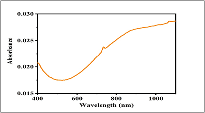
Fig. 2.UV–Visible absorbance spectrum of hydrothermally synthesized CuO
thin film recorded in the wavelength range of 400–1100 nm.
The optical band gap energy of the CuO thin film was estimated using the Tauc relation, assuming a direct allowed transition:(αhν)2=A(hν−Eg). The plot of (αhν) 2versus photon energy (hν) is shown in Fig. 3. A clear linear region is observed in the higher photon energy range (3.6–3.8 eV), indicating the onset of strong interband optical absorption
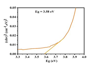
Fig. 3. The graph of (αhν) 2versus photon energy for hydrothermally
Synthesized CuO thin film showing a direct optical band gap of 3.58 eV.
By extrapolating the linear portion of the curve to the energy axis at (αhν) 2= 0, the optical band gap energy of the CuO thin film is determined to be 3.58 eV. The deviation from linearity at lower photon energies can be attributed to band tailing effects caused by localized defect states and structural disorder in the film. The relatively wide band gap suggests high optical transparency in the visible region and strong absorption in the ultraviolet region. Such characteristics are desirable for applications in UV photodetectors, transparent optoelectronic devices, and window layers in photovoltaic systems.
The electrical transport properties of the hydrothermally synthesized CuO thin film were examined through current–voltage (I–V) measurements at room temperature. The I–V characteristics of the film are presented in Fig. 4, with the applied voltage varied from 0 to 14 V.The I–V curve exhibits a nearly linear relationship between current and applied voltage, indicating ohmic conduction behavior. This linearity suggests good electrical contact between the electrodes and the CuO thin film, as well as uniform film thickness and improved grain connectivity. The absence of current saturation or rectifying behavior implies minimal barrier formation at the electrode–film interface.
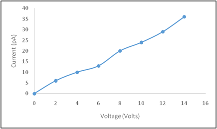
Fig. 4. Current–voltage (I–V) characteristics of hydrothermally synthesized
CuO thin film measured at room temperature.
The observed electrical behavior confirms the semiconducting nature of the CuO thin film and demonstrates efficient charge carrier transport. The hydrothermal synthesis method contributes to improved crystallinity and reduced interfacial resistance, resulting in stable electrical performance suitable for device applications.
The optical and electrical studies reveal a strong correlation between the structural quality and functional performance of the CuO thin film. The wide optical band gap of 3.58 eV ensures high transparency in the visible region, while the linear I–V characteristics confirm efficient charge transport across the film. Although defect states introduced during hydrothermal synthesis influence the optical absorption behavior, they do not significantly deteriorate the electrical conductivity, indicating an optimal balance between optical and electrical properties.
The hydrothermal method plays a crucial role in controlling the growth and properties of CuO thin films. The controlled temperature and pressure conditions promote uniform nucleation, enhanced crystallinity, and strong adhesion to the substrate. These factors collectively contribute to the observed optical transparency, well-defined band gap, and ohmic electrical behavior. The results demonstrate that hydrothermal synthesis is an effective and reliable technique for producing high-quality CuO thin films for optoelectronic applications.
4. Conclusion
In the present study, CuO thin films were successfully synthesized using a simple and cost-effective hydrothermal method and systematically investigated for their optical and electrical properties. The hydrothermal growth process enabled the formation of uniform, well-adhered CuO thin films with favorable optoelectronic characteristics.
UV–Visible spectroscopic analysis revealed moderate absorption in the visible region with enhanced absorption toward the near-infrared region. The optical band gap, determined using the Tauc method, was found to be 3.58 eV, which is higher than that of bulk CuO. This widening of the band gap is attributed to nanoscale effects, defect-induced band tailing, and structural disorder introduced during hydrothermal synthesis and post-annealing treatment. The wide band gap indicates high transparency in the visible region, making the films suitable for ultraviolet-based optoelectronic applications.
Electrical characterization demonstrated a nearly linear current–voltage relationship, confirming ohmic conduction behavior and efficient charge transport across the film. The absence of rectifying behavior suggests good electrical contact and uniform film morphology, which are essential for reliable device performance.
Overall, the combined optical and electrical analyses confirm that the hydrothermal synthesis route is an effective and scalable technique for producing high-quality CuO thin films. The wide optical band gap, stable electrical response, and low-cost fabrication process highlight the potential of hydrothermally grown CuO thin films for applications in UV photodetectors, transparent electronics, optoelectronic devices, and photovoltaic window layers.
5.Acknowledgements
The authors are grateful to the Principal of S. G. Patil Arts, Science and Commerce College, Sakri, Dist-Dhule for providing laboratory facilities and experimental support to carry out this research work. The authors also acknowledge the support extended by S.S.V.P. S’s L.K. Dr. P. R. Ghogrey Science College, Dhule,for their cooperation and academic encouragement.
The authors sincerely thank the technical staff of the participating institutions for their assistance during thin-film synthesis and electrical and optical characterization. The authors declare that no external funding was received for this work.
References.
- Ü. Özgür, Y. I. Alivov, C. Liu, et al., “A comprehensive review of ZnO materials and devices,” J. Appl. Phys., vol. 98, no. 4, p. 041301, 2005.
- S. J. Pearton, D. P. Norton, K. Ip, Y. W. Heo, and T. Steiner, “Recent advances in processing of ZnO,” Prog. Mater. Sci., vol. 50, pp. 293–340, 2005.
- J. B. Goodenough, “Electronic and ionic transport properties and other physical aspects of perovskites,” Rep. Prog. Phys., vol. 67, pp. 1915–1960, 2004.
- A. Rogalski, “Infrared detectors: status and trends,” Prog. Quantum Electron., vol. 27, pp. 59–210, 2003.
- M. H. Fulekar, Nanotechnology: Importance and Applications, I. K. International Publishing House, New Delhi, 2010.
- S. B. Ogale, Thin Films and Heterostructures for Oxide Electronics, Springer, Berlin, 2005.
- R. Chandrasekaran, S. Jayakumar, and M. G. Krishna, “Structural, optical and electrical properties of CuO thin films,” J. Mater. Sci.: Mater. Electron., vol. 25, pp. 152–158, 2014.
- C. J. Brinker and G. W. Scherer, Sol–Gel Science: The Physics and Chemistry of Sol–Gel Processing, Academic Press, New York, 1990.
- S. Major, S. Kumar, M. Bhatnagar, and K. L. Chopra, “Effect of hydrogen plasma treatment on transparent conducting oxides,” Thin Solid Films, vol. 122, pp. 31–36, 1985.
- P. K. Ghosh, S. K. De, and S. Chaudhuri, “CuO thin films deposited by magnetron sputtering,” Surf. Coat. Technol., vol. 206, pp. 123–129, 2011.
- J. Morales, L. Sánchez, F. Martín, J. R. Ramos-Barrado, and M. Sánchez, “Thermal oxidation synthesis of CuO nanostructures,” Electrochim. Acta, vol. 50, pp. 2039–2044, 2005.
- A. Phuruangrat, T. Thongtem, and S. Thongtem, “Synthesis of CuO nanostructures by precipitation method,” Mater. Lett., vol. 63, pp. 1537–1539, 2009.
- K. Byrappa and M. Yoshimura, Handbook of Hydrothermal Technology, William Andrew Publishing, New York, 2001.
- K. Byrappa and T. Adschiri, “Hydrothermal technology for nanotechnology,” Prog. Cryst. Growth Charact. Mater., vol. 53, pp. 117–166, 2007.
- M. Yoshimura and K. Byrappa, “Hydrothermal processing of materials: past, present and future,” J. Mater. Sci., vol. 43, pp. 2085–2103, 2008.
- R. E. Riman, W. L. Suchanek, and K. Byrappa, “Solution synthesis of ceramics,” Annu. Rev. Mater. Sci., vol. 32, pp. 377–407, 2002.
- S. Jana, A. K. Srivastava, and S. P. Singh, “Size dependent optical properties of CuO nanoparticles,” J. Alloys Compd., vol. 509, pp. 9809–9815, 2011.
- H. Raebiger, S. Lany, and A. Zunger, “Origins of p-type conductivity in Cu₂O,” Phys. Rev. B, vol. 76, p. 045209, 2007.
- A. Al-Amri, A. S. Al-Tuwirqi, A. A. Al-Ghamdi, and F. Yakuphanoglu, “Optical properties of Ni-doped CuO nanoparticles,” Physica B, vol. 407, pp. 2497–2501, 2012.
- A. M. Abd-Elnaiem, M. M. Rashad, and H. H. Afify, “CuO nanowires for photocatalytic applications,” Appl. Surf. Sci., vol. 258, pp. 8171–8176, 2012.
- D. Giziński, A. Lisowska-Oleksiak, and M. Gazda, “CuO as electrode material for electrochemical applications,” Electrochim. Acta, vol. 104, pp. 94–101, 2013.
- RoaaA.Abaas,EvanT.Salim,RanaO.Mahdi, “ASightofViewonHydrothermalSynthesisofCopperOxide”, EngineeringandTechnologyJournal41 (04),592-602, 2023.

You must be logged in to post a comment.