
Bharat G. Thakare1, Niranjan S. Samudre1, Amol R. Naikda1, Navnath M. Yajgar1, Bhushan B. Chaudhari1, Sudam D. Chavhan1*, R. R. Ahire1, Sachin J. Nandre2*,
1 Department of Physics, S. G. Patil Art’s, Science and Commerce College, Sakri (Maharashtra)
2 Department of Physics, U. P. College, Dahivel (Maharashtra)
*Email: – sachinjnandre@gmail.com , sudam1578@gmail.com
Abstract
This study explores the optoelectronic properties of Sb₂Se₃ thin films grown via chemical bath deposition (CBD), selenosulphate solution prepared by refluxing method, alongside antimony potassium tartrate solution complexed with triethanolamine and ammonia, diluted to 100 mL. Clean glass substrates underwent room-temperature deposition for 4 hours in darkness to ensure controlled nucleation, followed by rinsing with deionized water, drying hot air using dryer. Optical and electrical properties of chemically deposited Sb₂Se₃ thin films were systematically investigated to assess their suitability. Transmittance analysis in the wavelength range of 500–1000 nm reveals moderate transparency (~35–40%) in the near-infrared region, while a sharp decrease in transmittance below ~800 nm indicates a distinct absorption edge. Correspondingly, the absorbance spectrum exhibits strong absorption in the visible region (500–700 nm), confirming efficient photon harvesting with absorption coefficients exceeding 10⁴–10⁵ cm⁻¹. The optical bandgap, determined using a Tauc plot for direct allowed transitions, is found to be approximately 1.4 eV, which lies within the optimal range for single-junction solar cell applications. Electrical characterization of the as-deposited films shows linear and symmetric I–V behavior with current increasing from 0 to ~35 pA over 0–14 V, indicating ohmic conduction dominated by high series resistance. This behavior is attributed to intrinsic film resistance arising from amorphous regions, selenium vacancies, and poor inter-grain connectivity typical of unannealed solution-grown films. The absence of rectifying characteristics suggests an incomplete photovoltaic device lacking a p–n junction. Post-deposition treatments such as annealing or selenization are expected to improve crystallinity, reduce defect density, and enable efficient charge collection for enhanced solar cell performance.
Keywords: –Reflux; TEA; Sb2Se3; CBD; Optical; I-V.
Introduction
The rapid growth of optoelectronic and photovoltaic technologies has intensified the search for efficient, low-cost, and environmentally benign semiconductor materials. In this context, antimony selenide (Sb₂Se₃) has emerged as a promising absorber material owing to its suitable band gap, high optical absorption coefficient, and favorable charge transport properties [1]. Sb₂Se₃ is a V–VI compound semiconductor composed of earth-abundant and non-toxic elements [2,3], which makes it attractive for sustainable large-scale optoelectronic applications.Sb₂Se₃ crystallizes in an orthorhombic structure consisting of one-dimensional (Sb₄Se₆)ₙ ribbons held together by van der Waals forces. This unique structural arrangement leads to strong anisotropy in optical and electrical properties and contributes to efficient light absorption and carrier transport along preferred crystallographic directions [4,5]. The material exhibits a direct band gap in the range of 1.1–1.3 eV and an absorption coefficient exceeding 10⁵ cm⁻¹ in the visible region, which is well suited for solar energy harvesting and photodetection devices [6].The optoelectronic properties of Sb₂Se₃ thin films are highly dependent on the deposition technique and growth parameters. Various vacuum-based methods such as thermal evaporation, sputtering, and vapor transport deposition have been employed to fabricate Sb₂Se₃ films with controlled properties [7, 8]. However, these methods often involve high processing temperatures, complex instrumentation, and increased fabrication costs. Consequently, solution-based deposition techniques have attracted considerable interest as viable alternatives due to their simplicity, low energy consumption, and potential for large-area and flexible substrates [9].Solution growth methods, including chemical bath deposition, hydrothermal synthesis, and spin coating, offer enhanced control over film morphology, stoichiometry, and thickness through optimization of precursor concentration, bath temperature, deposition time, and solution chemistry [10, 11, 12]. These parameters play a crucial role in determining the optical absorption behavior, band gap energy, carrier concentration, and electrical conductivity of Sb₂Se₃ thin films. Systematic optoelectronic studies of solution-grown Sb₂Se₃ are therefore essential to establish correlations between growth conditions and functional properties.In view of these considerations, the present study focuses on the optoelectronic investigation of solution-grown Sb₂Se₃ thin films. Detailed analysis of optical properties such as absorbance, transmittance, and band gap energy, along with electrical characteristics, provides valuable insight into the potential of these films for optoelectronic and photovoltaic applications [13, 14, 15]. Understanding and optimizing these properties is a key step toward the development of efficient, low-cost Sb₂Se₃-based devices.
Experimental Work
Materials. Antimony Potassium Tartrate Hemihydrate (C4H4O7KSb.1/2H2O; Extra pure AR, 99.5%-Sisco Research Laboratories Pvt. Ltd.), Selenium Metal Pellets (Se 99.999%), Sodium Sulphite Anhydrous (Na2SO3; AR-98%), Triethanolamine (C6H15NO3; Extra pure 98%), Ammonia Solution (NH4OH; Extra pure 30%), Acetone and Isopropanol Loba Chemie Pvt. Ltd. were used as precursors, reducing agents, complexing agents, and pH adjusters, respectively. Acetone and Isopropanol Loba Chemie Pvt. Ltd.) served as solvents for substrate cleaning and post-deposition rinsing. All chemicals were used as received without further purification.
Synthesis of Sb2Se3
Soda-lime glass substrates (dimensions: 75 mm × 25 mm × 1 mm) were meticulously cleaned prior to deposition to ensure a contamination-free surface[16]. The cleaning protocol involved sequential ultrasonic treatment in the following sequence: (i) a mild detergent solution (e.g., Labolene) for 5 min to remove organic residues; (ii) double-distilled water for 5 min; (iii) ethanol (99.9% purity) for 5 min; and (iv) isopropanol (99.7% purity) for 5 min. After each ultrasonication step, substrates were thoroughly rinsed with copious amounts of DDW to eliminate residual contaminants and prevent cross-contamination. The cleaned substrates were then dried using a gentle nitrogen gas blow to minimize particulate redeposition, followed by UV-ozone treatment for 10 minutes to enhance surface hydrophilicity and remove any remaining adventitious carbon. Finally, the prepared substrates were stored in a dust-free laminar flow cabinet until use for thin film deposition.The selenide source, 0.4 M sodium selenosulphate solution, was synthesized by refluxing 100 mL of 1 M sodium sulfite solution with excess selenium metal pellets (Se, 99.999% purity) at 90°C for 6 hours under constant stirring, adapting the procedure reported by Rodriguez-Lazcano et al. [17]. In a separate 100 mL beaker, 0.12 M of antimony potassium tartrate hemihydrate was dissolved in 32 mL of DDW with magnetic stirring until a homogeneous clear solution. To this, 3 mL of triethanolamine was added as a complexing agent, followed by 15 mL of 30% ammonia solution to adjust pH and stabilize the Sb-complex. The mixture was stirred vigorously for 10 minutes. Subsequently, 12 mL of the freshly prepared 0.2 M solution was introduced dropwise, and DDW was added to adjust the total volume to 100 mL, yielding the final chemical bath deposition (CBD) precursor solution.Cleaned glass substrates were vertically immersed in the chemical bath with the bath covered in aluminium foil to prevent photodegradation of the selenosulphate precursor. The deposition was conducted in a dark environment at room temperature (24 °C) for 4 hours to promote controlled nucleation and growth of the Sb₂Se₃ thin film via the CBD mechanism. Upon completion, the substrate was gently removed from the bath and rinsed thoroughly with DDW to wash away loosely adhered particles, residual precursors, and byproducts. The film was initially dried using a hot air dryer at 60°C, followed by purging with high-purity nitrogen gas to ensure uniform drying without mechanical damage.The processed substrate was allowed optical, and electrical characterization.
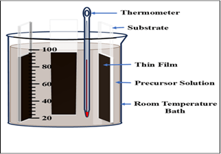
Fig. 1 Experimental Set-up of CBD at
room temperature
Result and Discussion: The Fig. 2 (a) plots transmittance (%) on the y-axis (0–40%) against wavelength (nm) on the x-axis (500–1000 nm), with a blue curve labeled “Sb₂Se₃”. The film shows moderate transparency starting at ~35–40% around 900–1000 nm in the near-infrared (NIR) region, where longer wavelengths pass through with minimal absorption. As wavelength decreases toward the visible range (500–800 nm), transmittance drops sharply from ~30% at 850 nm to near 0% below 700 nm, indicating a distinct absorption edge. This behaviour reflects the fundamental absorption process where photons with energy exceeding the bandgap (~1.5 eV, corresponding to ~825 nm) are strongly absorbed, while lower-energy NIR photons transmit—ideal for top-cell applications in tandem solar cells or single-junction devices targeting AM1.5G spectrum utilization.Directly adjacent Fig. 2 (b) absorbance (arbitrary units, 0–1.4) versus wavelength (500–1000 nm) is shown in red (“Sb₂Se₃”),
displaying the inverse trend: near-zero absorbance beyond 900 nm, followed by a steep rise commencing around 800 nm. Peak absorbance (>1.2 units) occurs in the 500–700 nm visible range, plateauing at high values that imply absorption coefficients (α) exceeding 10⁴–10⁵ cm⁻¹—characteristic of direct bandgap chalcogenides like Sb₂Se₃. This profile confirms efficient photon capture from blue-green to red light, with the onset aligning precisely with the transmittance edge, as expected from the Beer-Lambert law (T = e^{-αd}, where d is film thickness, typically 200–1000 nm for chemical bath deposited films).The Fig. 2 (c)employs a Tauc representation for direct allowed transitions, plotting (αhν)² (units: cm⁻² eV², 0–3) versus photon energy (hν, 1.2–1.8 eV) in green (“Sb₂Se₃, Eg=1.4 eV”). Here, α is derived from absorbance via α = (ln(1/T))/d, assuming uniform thickness. The curve remains flat near zero below ~1.4 eV (sub-bandgap scattering), then rises linearly with a steep slope above 1.4 eV, characteristic of direct interband transitions described by the Tauc equation: (αhν)² = A(hν – Eg), where A is a constant and Eg is the optical bandgap. Extrapolating the linear portion (tangent from ~1.45–1.65 eV) intersects the x-axis at precisely 1.4 eV, confirming the film’s direct bandgap. This value falls within the optimal range (1.1–1.6 eV) for single-junction photovoltaics. The I-V characteristic of as-deposited Sb₂Se₃ thin films, shown in Fig. 2 (d)the attached plot, displays linear ohmic behavior with current increasing steadily from 0 mA at 0 V to approximately 35 mA at 14 V, reflecting symmetric conduction without rectification. This indicates high series resistance dominated by the intrinsic absorber layer—typical for unannealed chemical bath deposited films featuring amorphous regions, Se vacancies, and poor inter-grain contacts that limit charge transport. For photovoltaic applications, such ohmic response signals an incomplete device lacking a p-n junction (e.g., with n-CdS), as ideal solar cells require diode-like rectification to generate Voc, Jsc, and fill factor under illumination; annealing or selenization treatments typically enhance crystallinity, reduce defects, and enable carrier collection along the ribbon-like structure for efficiencies reaching 3-10%.[18, 19, 20]
Conclusion
In summary, this work successfully demonstrated a reproducible chemical bath deposition route for Sb₂Se₃ thin films using in-house sodium selenosulphate and antimony potassium tartrate precursors, yielding uniform coatings at room temperature with controlled post-processing. Optical spectra confirmed strong visible absorption (α > 10⁴ cm⁻¹), NIR transparency (35-40%), and a direct bandgap of 1.4 eV-optimally matched to AM1.5G illumination for photovoltaic absorbers—while the linear ohmic I-V response highlighted intrinsic high resistivity from defects in as-deposited films, underscoring the need for annealing to form rectifying junctions and boost carrier collection. These findings validate solution-processing viability for low-cost Sb₂Se₃ optoelectronics, paving the way for tandem cell integration and efficiency gains beyond 10% through targeted defect passivation and texturing.
Acknowledgements
One of the authors, Mr. Bharat Thakare, expresses sincere gratitude to the Trible Research and Training Institute, Pune, for financial support through a Maharashtra Government-sponsored fellowship during his Ph.D. research. The authors also extend their heartfelt thanks to the Principal of S.G. Patil ASC College, Sakri, for providing access to essential research facilities and infrastructure that enabled this work.
References
- Ying Zhou, Liang Wang, Shiyou Chen, Sikai Qin, Xinsheng Liu, Jie Chen, Ding-Jiang Xue, Miao Luo, Yuanzhi Cao, Yibing Cheng, Edward H. Sargent & Jiang Tang, Thin-film Sb₂Se₃ photovoltaics with oriented one-dimensional ribbons, Nature Photonics, vol. 9, pp. 409–415, 2015
- Majidzade, Vusala A. “Sb2Se3-based solar cells: obtaining and properties.” Kimya Problemleri 2 (2020): 181-198.
- Vidal Fuentes, Pedro. “Quasi One Dimensional Antimony Selenide Thin Film Solar Cells for Next Generation Photovoltaics.” (2022).
- Zhugayevych, Andriy, Olena Postupna, Ronald C. Bakus II, Gregory C. Welch, Guillermo C. Bazan, and Sergei Tretiak. “Ab initio study of a molecular crystal for photovoltaics: Light absorption, exciton and charge carrier transport.” The Journal of Physical Chemistry C 117, no. 10 (2013): 4920-4930.
- Wang, Manjing, Sanlong Wang, Qixing Zhang, Sanjiang Pan, Ying Zhao, and Xiaodan Zhang. “Controlling the crystallographic orientation of Sb2Se3 film for efficient photoelectrochemical water splitting.” Solar RRL 6, no. 4 (2022): 2100798.
- Stroyuk, Oleksandr, Alexandra Raevskaya, and Nikolai Gaponik. “Solar light harvesting with multinary metal chalcogenide nanocrystals.” Chemical Society Reviews 47, no. 14 (2018): 5354-5422.
- Luo, Yandi. “Development of new buffer layers and rapid annealing process for efficient Sb2Se2 thin-film solar cells.” PhD diss., Université de Rennes, 2024.
- Vishwanathan Vidyanagar, Akshay, Stenny Benny, and SarpangalaVenkataprasad Bhat. “Antisolvent Treatment for Antimony Selenide Thin Film Augmenting Optoelectronic Performance.” Advanced Optical Materials 13, no. 17 (2025): 2500175.
- Zhang, Yaokang, Sze-Wing Ng, Xi Lu, and Zijian Zheng. “Solution-processed transparent electrodes for emerging thin-film solar cells.” Chemical reviews 120, no. 4 (2020): 2049-2122.
- Veeramalai, Chandrasekar Perumal, Yang Xu, Yuquan Chen, Guochen Lin, Jing Wang, Yang Wang, Chuanbo Li, and Xiaoming Zhang. “Photoelectronic properties of antimony selenide nanowire synthesized by hydrothermal method.” Colloids and Surfaces A: Physicochemical and Engineering Aspects 674 (2023): 131889.
- Yuqi Zhao, Shaoying Wang, Chuang Li, Bo Che, Xueling Chen, Hongyi Chen, Rongfeng Tang, Xiaomin Wang, Junbo Gong, Tao Chen, Guilin Chen, Xudong Xiao and Jianmin Li, “Regulating deposition kinetics via a novel additive-assisted chemical bath deposition technology enables fabrication of 10.57% efficiency Sb2Se3 solar cells.” Energy Environ. Sci., 2022, 15, 5118.
- Luo, Yandi, Guojie Chen, Shuo Chen, Nafees Ahmad, Muhammad Azam, Zhuanghao Zheng, Zhenghua Su et al. “Carrier transport enhancement mechanism in highly efficient antimony selenide thin‐film solar cell.” Advanced Functional Materials 33, no. 14 (2023): 2213941.
- Bai, Hang, Yufang Li, Honglie Shen, Long Wang, Hechao Li, Zhihong Xie, Andi Chen, Zheng Shi, and Wei Wang. “Preparation of antimony selenide thin films by electrochemical deposition and application in optoelectronic devices.” Materials Science in Semiconductor Processing 171 (2024): 108027.
- Nadukkandy, Aiswarya, Sadasivan Shaji, David Avellaneda Avellaneda, Josue Amilcar Aguilar-Martinez, and Bindu Krishnan. “Cubic structured silver antimony sulfide-selenide solid solution thin films for sustainable photodetection and photovoltaic application.” Journal of Alloys and Compounds 942 (2023): 169072.
- Chen, Guojie, Shuo Chen, Jun Zhao, Zhenghua Su, and Guangxing Liang. “Advances in optoelectronic applications of antimony chalcogenide thin films.” Nano Research 18, no. 10 (2025): 94907931.
- Bhattacharyya, Dhiman, Wei Hong, Kay Peng, and Vincent Sih. “Reduction of extra pattern defects in immersion layer reworks by cleans recipe optimization: CFM: Contamination free manufacturing.” In 2016 27th Annual SEMI Advanced Semiconductor Manufacturing Conference (ASMC), pp. 229-232. IEEE, 2016.
- Y. Rodrı´guez-Lazcano, Yolanda Pen˜a, M.T.S. Nair, P.K. Nair, Polycrystalline thin films of antimony selenide via chemical bath deposition and post deposition treatments, Thin Solid Films 493 (2005) 77– 82.
- Zhao, Qi, Rongfeng Tang, Shangfeng Yang, and Tao Chen. “Post‐Treatment Strategies Toward High‐Quality Sb2Se3 Thin Films in Photovoltaic Applications.” Advanced science 12, no. 36 (2025): e11387.
- He, Haiying, Yiming Zhong, Wanying Zou, Xinyu Zhang, Jun Zhao, Muhammad Ishaq, and Guangxing Liang. “A novel Se-diffused selenization strategy to suppress bulk and interfacial defects in Sb2Se3 thin film solar cell.” Surfaces and Interfaces 51 (2024): 104793.
- Sindi, Daniya. “Optimization of Close Space Sublimation and Post Deposition Routes for Antimony Chalcogenide Solar Cells.” PhD diss., University of Liverpool, 2025.


You must be logged in to post a comment.